Comparison Asus GeForce RTX 5070 Ti Prime OC vs MSI GeForce RTX 4070 Ti SUPER 16G VENTUS 3X OC
Add to comparison | 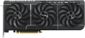 |  |
|---|---|---|
| Asus GeForce RTX 5070 Ti Prime OC | MSI GeForce RTX 4070 Ti SUPER 16G VENTUS 3X OC | |
| Compare prices 11 | from $829.99 | |
| User reviews | ||
| TOP sellers | ||
| Interface | PCIe v5.0 16x | PCIe v4.0 16x |
GPU | ||
| Model GPU | GeForce RTX 5070 Ti | GeForce RTX 4070 Ti SUPER |
| Architecture | Blackwell | Ada Lovelace |
| Memory size | 16 GB | 16 GB |
| Memory type | GDDR7 | GDDR6X |
| Memory bus | 256 bit | 256 bit |
| Nominal frequency (Core Clock) | 2497 MHz | |
| Maximum frequency (Boost Clock) | 2527 MHz | 2655 MHz |
| Memory speed | 28000 Mbps | 21000 Mbps |
| Lithography | 4 nm | 5 nm |
| Max. resolution | 7680x4320 px | 7680x4320 px |
Connections | ||
| HDMI | 1 | 1 |
| HDMI version | v2.1b | v2.1a |
| DisplayPort | 3 | 3 |
| DisplayPort version | v.2.1b | v.1.4a |
Software | ||
| DirectX | 12 Ultimate | 12 Ultimate |
| OpenGL | 4.6 | 4.6 |
| Stream processors | 8960 | 8448 |
| Tensor cores | 280 | |
| RT nuclear | 70 | |
| Texture units | 280 | |
| Passmark G3D Mark test | 31326 points | 32032 points |
General | ||
| Monitors connection | 4 | 4 |
| Cooling | active (fan) | active (fan) |
| Fans | 3 pcs | 3 pcs |
| Power consumption | 300 W | 285 W |
| Additional power | 16 pin | 16 pin |
| Minimum PSU recommendation | 750 W | 700 W |
| Length | 306 mm | 308 mm |
| Height | 126 mm | 120 mm |
| Occupies slots | 2.5 | 2.5 |
| Added to E-Catalog | january 2025 | january 2024 |
Compare Asus GeForce RTX 5070 Ti Prime OC and MSI GeForce RTX 4070 Ti SUPER 16G VENTUS 3X OC
You may be interested in
Asus GeForce RTX 5070 Ti Prime OC often compared


Glossary
Interface
The interface through which a video card connects to a computer's motherboard.
In fact, the standard interface for modern video cards is PCIe (PCI Express of various versions: PCIe v2.0, PCIe v3.0, PCIe v4.0, PCIe v5.0); it has almost completely replaced the outdated AGP and "regular" PCI. Different versions and different numbers of PCIe lanes can be provided in modern components; for video cards, the compatibility rules with motherboards are as follows:
1. The number of PCIe lanes in the motherboard slot should be no less than the number of lanes on the video card. For example, a PCIe x8 video adapter can be connected to a PCIe x16 slot, but not the other way around. Generally, it's reasonable to assume that the connection will require an x16 slot: this is the maximum number of lanes found in motherboard slots, and it's what most modern video cards require to achieve the necessary bandwidth.
2. A video card of an older PCIe version can be connected to a slot of a newer version; however, the opposite is usually not possible (with rare exceptions—PCIe v2.1 video adapters may work on some cards with v2.0 slots, but this possibility should be clarified separately).
As for specific PCIe versions, the options can be:
— PCIe v2.0. The earliest of the currently relevant PCI Express versions. The bandwidth of one line of this inte...rface is 5 GT/s (gigatransactions per second), which in practice gives 500 MB/s per line. Consequently, the maximum data transfer speed (with 16 lanes) reaches 8 GB/s in each direction.
— PCIe v2.1. An improved version of 2.0 with some software enhancements; in terms of hardware and bandwidth, it is completely identical to its predecessor.
— PCIe v3.0. A fundamental update to the PCIe standard, featuring a more advanced data encoding scheme—128b/130b, meaning 2 "extra" bits for every 128 bits of useful information (while earlier standards used 8b/10b, with 2 service bits for every 8 main ones). Thanks to this, data transfer speed almost doubled compared to its predecessor (up to 985 MB/s per line), while the number of transactions increased from 5 to 8 GT/s.
— PCIe v4.0. A further development of the PCIe standard described above, released to the market in 2019. Compared to the previous version 3.0, the bandwidth was doubled again—to 16 gigatransactions per second (1969 MB/s per line, 31.5 GB/s on x16).
— PCIe v5.0. The 2025 standard compared to PCIe 4.0 doubles the bandwidth, providing up to 32 GT/s per line and up to 128 GB/s in x16 mode, which is particularly useful for data-intensive tasks such as rendering, machine learning, and ray tracing. This improvement unleashes the potential of next-generation high-performance graphics cards and ensures fast work with large amounts of data, although the difference is still minimal for gaming. PCIe 5.0 also retains backward compatibility, making it convenient for integration into modern systems.
Model GPU
A GPU is a type of graphics processor that determines the fundamental performance characteristics of a video adapter. Today there are two main manufacturers - AMD and NVIDIA. Intel has also entered the leadership race with its Intel Arc (A-Series, B-Series) line of discrete graphics.
NVIDIA: GeForce GT 1030, GeForce GTX 1050 Ti, GeForce GTX 1060, GeForce GTX 1070, etc. (all related to GeForce 10 series), GeForce GTX 1630, GeForce GTX 1650( SUPER), GeForce GTX 1660( SUPER, Ti), GeForce RTX 20 series, namely GeForce RTX 2060( SUPER), GeForce RTX 2070( SUPER), GeForce RTX 2080( SUPER, Ti), GeForce RTX 3050, GeForce RTX 3060..., GeForce RTX 3060 Ti, GeForce RTX 3070, GeForce RTX 3070 Ti, GeForce RTX 3080, GeForce RTX 3080 Ti, GeForce RTX 3090, GeForce RTX 3090 Ti, GeForce RTX 4060, GeForce RTX 4060 Ti, GeForce RTX 4070, GeForce RTX 4070 SUPER, GeForce RTX 4070 Ti, GeForce RTX 4 070 Ti SUPER, GeForce RTX 4080, GeForce RTX 4080 SUPER, GeForce RTX 4090, GeForce RTX 5050, GeForce RTX 5060, GeForce RTX 5060 Ti, GeForce RTX 5070, GeForce RTX 5070 Ti, GeForce RTX 5080, GeForce RTX 5090, as well as professional Quadro.
AMD: Radeon RX 500 series as Radeon RX 550, Radeon RX 560, Radeon RX 570, Radeon RX 580, Radeon RX 590, Radeon RX 5500 XT, Radeon RX 5600 XT, Radeon RX 5700, Radeon RX 5700 XT, Radeon RX 6400, Radeon RX 6500 XT, Radeon RX 6600, Radeon RX 6600 XT, Radeon RX 6650 XT, Radeon RX 6700 XT, Radeon RX 6750 XT , Radeon RX 6800, Radeon RX 6800 XT, Radeon RX 6900 XT, Radeon RX 6950 XT, Radeon RX 7600, Radeon RX 7600 XT, Radeon RX 7700 XT, Radeon RX 7800 XT, Radeon RX 7900 XT, Radeon RX 7900 XTX, Radeon RX 7900 GRE, Radeon RX 9060 XT, Radeon RX 9070, Radeon RX 9070 XT, Radeon RX Vega 56, Radeon RX Vega 64, AMD Radeon VII and professional FirePro.
Knowing the GPU model, you can find detailed information on it (special specs, reviews, reviews, etc.) and evaluate how suitable this board is for your purposes. It is worth noting that in video cards from third-party brands, the characteristics of the graphics processor may differ slightly from the standard ones (and often in the direction of acceleration and improvement).
Architecture
A set of properties and qualities inherent in a whole family of video cards. The GPU architecture is designed for massively parallel computing to efficiently handle computer graphics processing.
Modern video cards are built according to one of several common architectures:
Turing. The NVIDIA Turing architecture debuted towards the end of 2018. It is named after the English mathematician Alan Turing. Turing has pioneered ray tracing RT cores that accelerate light and sound motion calculations in a 3D environment by up to 10 billion rays per second. Also, the architecture is equipped with tensor cores, a new multi-threaded processor and a unified cache architecture with double the bandwidth (compared to previous generations). Used by Turing in GeForce RTX, Quadro RTX and Tesla T4 graphics cards.
Ampere. The second generation RTX architecture that replaced Turing in 2020. It is named after the French physicist and mathematician André-Marie Ampère. The architecture marked the rise of the NVIDIA GeForce RTX 3000 series gaming graphics cards. Ampere introduced new streaming multiprocessors, second edition RT cores, and third generation tensor cores. The key point of these improvements is not only an increase in raster performance, but also a reduction in the load when calculating rays. The Ampere architecture is found in the GeForce 30 family of...GPUs from NVIDIA.
Ada Lovelace. Launched in 2021, the Ada Lovelace family of GPUs features new 3G RT cores that provide 2x performance gains with ray tracing. The architecture also uses fourth-generation tensor cores, which are up to two times faster in AI training operations, and CUDA cores, which are twice as productive in single-precision operations compared to previous generation solutions. The architecture is implemented in NVIDIA GeForce 4000 and 6000 series video cards.
Navi (RDNA). The first graphics solutions from AMD based on the Navi RDNA architecture were released in the summer of 2019. Having half the area of the chip, it managed to accommodate the same 12.5 billion transistors as in the previous generation of chips on Vega 10. Video cards based on the Navi architecture (RDNA) video cards have increased energy efficiency and performance, especially in games. The debut of the architecture took place in the graphics cards of the Radeon RX 5700 line.
Big Navi (RDNA 2). Big Navi Architecture (RDNA 2) has been on the move since 2020. She got improved computing units, an improved graphics pipeline and a new high-speed cache memory AMD Infinity Cache. The architecture demonstrates high levels of energy efficiency and performance. In particular, compared with the first edition of RDNA, the increase in performance per watt was up to 54%. Also, Big Navi has improved hardware devices for ray tracing (Ray Accelerator), which provides more realistic rendering of graphics in demanding games. The architecture is used in AMD Radeon RX 6000 series video cards and top gaming consoles (Sony PlayStation 5, Xbox S/X).
Navi 3X (RDNA 3). Changes in the third edition of the RDNA architecture are aimed at comprehensively improving gaming performance at high resolutions of 4K and 8K. RDNA 3-based GPUs are the first multi-chip GPUs from AMD. Redesigned compute units and second-generation AMD Infinity Cache technology deliver up to a 54% performance boost when compared to the previous generation Big Navi Navi 3X. There are also improvements in ray tracing performance - the corresponding blocks can count on 50% more rays per clock. The architecture has found application in gaming video cards of the AMD Radeon RX 7000 family.
Memory type
The type of graphics memory used by the graphics card (see GPU memory capacity). To date, the following types of memory are used:
— DDR3. General purpose RAM that is not specialized for graphics processing and was originally designed for use in the general system RAM. However, due to good performance and relatively low cost, it has recently been used in video cards (albeit, mainly at a low-cost level).
— DDR4. Further, after DDR3, the development of general-purpose RAM. Specifically, it is extremely rare in video cards, due to the prevalence of more advanced specialized standards.
— GDDR2. The second generation of memory built using Double Data-Rate technology (“double data transfer rate”). In fact, it is a modification of DDR2 RAM, optimized for use in video cards; just like the original DDR2, it provides 4 data transfer operations per cycle (original DDR — 2 operations). It has not received wide popularity due to the tendency to strong heating during operation.
— GDDR3. Improved version of GDDR2 (see above). It has a higher effective frequency (as a result, performance), while differing in lower heat dissipation. Some time ago it enjoyed considerable popularity, now it is gradually falling into disuse, giving way to more advanced standards.
— GDDR5. Pretty advanced video memory format; unlike earlier versions of GDDR...(see above), it is based on DDR3 RAM.
— GDDR5X. A further enhancement to GDDR5 memory designed to increase bandwidth (and thus overall speed and graphics performance). Various design improvements made it possible to achieve a 2-fold increase in maximum speed — up to 12 Gbps versus 6 Gbps for the original GDDR5. At the same time, although GDDR5X is inferior in terms of characteristics to HBM (see below), it is also much cheaper.
— GDDR6. Further, after GDDR5X, the development of GDDR-type graphic memory. Achieve data rates up to 16Gb/s per pin, nearly double that of GDDR5, at a lower operating voltage. Such characteristics allow the use of GDDR6 to work with 4K resolutions and higher, as well as virtual reality systems; video cards with such memory are mainly classified as top-end solutions.
— GDDR6X. An improved version of GDDR6 released in Fall 2020. According to the creators, it is the fastest graphics memory at the time of release. One of the key updates is the use of the so-called multi-level PAM4 modulation, which allows you to transfer 2 bits of data per cycle (versus 1 bit for its predecessors). Due to this, the bandwidth of GDDR6X can reach 21 Gbps per pin and 1 TB / s for the entire memory block (versus 16 Gbps and 700 Gbps, respectively, in the previous version). This type of memory is great even for the most powerful modern video cards, but it also costs accordingly.
— HBM. A type of memory designed to maximize throughput. It differs fundamentally from various versions of GDDR in that the HBM module is built on the "sandwich" principle — the memory chips in it are placed in layers and allow simultaneous access; and for communication with the processor, a special silicon layer is used, the so-called "interposer", which provides efficient transfer of large amounts of data. Due to this, HBM is significantly (many times) faster than even the most advanced versions of GDDR, and the clock frequency of such memory modules is low, which gives another advantage — extremely low power consumption and heat dissipation. The main disadvantage of this technology is its high cost.
— HBM2. The second generation of high-speed HBM memory, introduced in 2016. See above for more on the general features of HBM, and HBM2 has doubled throughput compared to the first version of this technology. Thanks to this, such memory is great for resource-intensive tasks like working with virtual reality.
Nominal frequency (Core Clock)
The core clock frequency, meaning the speed at which the GPU executes main computations during image processing. This parameter helps understand the overall performance level of the chip in games, 3D graphics, video editing, and other tasks where graphics performance is important. The higher the Core Clock, the more operations the video card can perform per unit of time under equal conditions. Along with it, Boost Clock is often indicated — this is the increased frequency, up to which the core can automatically overclock given appropriate temperature, power reserve, and settings.
Maximum frequency (Boost Clock)
The clock frequency of the GPU core, to which the GPU can automatically overclock under suitable conditions for temperature, cooling, and power supply. This parameter is necessary for the card to temporarily or quite long operate faster than the nominal level and deliver more performance in games, 3D graphics, and other heavy tasks.
The higher the Boost Clock, the more potential the graphics card has under load, especially in dynamic scenes where additional processing speed is important. However, this is not a constant value; it is the maximum or close to maximum operating mode, which depends on the specific system and the quality of cooling.
For example, in a game or during rendering, a graphics card with a high Boost Clock can noticeably more confidently maintain performance if the case is well ventilated and there is no overheating. Therefore, Boost Clock is particularly interesting for those choosing a model for gaming, editing, streaming, or other resource-intensive tasks.
Memory speed
Memory speed in graphics card specifications indicates how "quickly" the video memory operates and how fast the GPU can access and write data. It's similar to the concept of "bandwidth," but it's important not to confuse them: memory speed refers to the "rate" of the chips themselves, while the final bandwidth is also determined by the bus width. Thus, a card with slower memory but a wider bus can sometimes compete with a model that has faster memory and a narrower bus. Compared to core frequency, this parameter has a greater impact on scenarios with large textures and high resolution. If the graphics card has a large cache, the difference in memory speed may be less noticeable, as some data less frequently reaches VRAM. A typical example is enabling ultra-textures and 4K: if the memory speed is low, you might experience more drop-offs and load times, whereas with high memory speed, frames remain more stable and less "choppy" in demanding scenes.
Lithography
The process technology by which the graphics card's own processor is made.
This parameter is specified by the size of each individual transistor used in the processor. At the same time, the smaller this size, the more perfect the technical process is considered: reducing individual elements allows you to reduce heat dissipation, reduce the overall size of the processor, and at the same time increase its performance. Accordingly, nowadays, manufacturers are trying to move in the direction of reducing the technical process, and the newer the graphics card, the smaller the numbers in this paragraph can be.
This parameter is specified by the size of each individual transistor used in the processor. At the same time, the smaller this size, the more perfect the technical process is considered: reducing individual elements allows you to reduce heat dissipation, reduce the overall size of the processor, and at the same time increase its performance. Accordingly, nowadays, manufacturers are trying to move in the direction of reducing the technical process, and the newer the graphics card, the smaller the numbers in this paragraph can be.
HDMI version
HDMI interface version supported by the graphics card. For details about HDMI itself, see above, and its versions can be as follows:
— v.1.4. The earliest HDMI standard found in video cards; was introduced in 2009. Despite its “venerable age”, it has good capabilities: it supports 4K video (4096x2160) at a frame rate of 24 fps, Full HD (1920x1080) at a frame rate of up to 120 fps, and is also suitable for transmitting 3D video.
— v.1.4b. The second improvement of the above v.1.4. The first update, v.1.4a, introduced support for two additional 3D video formats; and in HDMI v.1.4b, mostly minor improvements and additions to v 1.4a specifications were implemented, almost imperceptible to the average user.
— v.2.0. Standard introduced in 2013 to replace HDMI v.1.4. Thanks to its full 4K support (up to 60 fps), it is also known as HDMI UHD. In addition, there is enough bandwidth for simultaneous transmission of up to 32 audio tracks and up to 4 separate audio streams, and the list of supported frame formats has been replenished with ultra-wide 21:9.
— v.2.0b. The second update of the HDMI 2.0 standard described above, which differs primarily in HDR support. However, HDR compatibility itself appeared in the first update, v.2.0a; and version 2.0b added the ability to work with HDR10 and HLG standards.
— v.2.1. The newest common HDMI standard released in 2017. Capable of providing a frame rate of 120 fps in ultra-high resolu...tion video signal — from 4K to 8K inclusive; some improvements related to the use of HDR were also provided. Note that all the features of HDMI v.2.1 are available only when using cables marked Ultra High Speed, although basic functions work through ordinary cables.